Artigo
| Ba-doped ZnO materials: a DFT simulation to investigate the doping effect on ferroelectricity |
|
Luis H. da S. Lacerda; Sergio R. de Lazaro*
Departamento de Química, Universidade Estadual de Ponta Grossa, 84030-900 Ponta Grossa - PR, Brasil Recebido em 30/07/2015 *e-mail: srlazaro@uepg.br ZnO is a semiconductor material largely employed in the development of several electronic and optical devices due to its unique electronic, optical, piezo-, ferroelectric and structural properties. This study evaluates the properties of Ba-doped wurtzite-ZnO using quantum mechanical simulations based on the Density Functional Theory (DFT) allied to hybrid functional B3LYP. The Ba-doping caused increase in lattice parameters and slight distortions at the unit cell angle in a wurtzite structure. In addition, the doping process presented decrease in the band-gap (Eg) at low percentages suggesting band-gap engineering. For low doping amounts, the wavelength characteristic was observed in the visible range; whereas, for middle and high doping amounts, the wavelength belongs to the Ultraviolet range. The Ba atoms also influence the ferroelectric property, which is improved linearly with the doping amount, except for doping at 100% or wurtzite-BaO. The ferroelectric results indicate the ZnO:Ba is an strong option to replace perovskite materials in ferroelectric and flash-type memory devices. INTRODUCTION Theoretical methods based on quantum mechanical simulations are an important tool to evaluate material properties, mainly at the molecular level. Studies based on these methods are performance to evaluate the electronic, optical, structural, pyro-, piezo- and ferroelectric properties. Such properties are intrinsically dependent on composition, atomic organization and chemical bonds, once these factors change the charge density on materials. One example is semiconductor materials, which are largely employed to develop electronic, optical devices, piezoelectric and memory devices.1-12 Actually, such devices are constructed using perovskite materials that have wide band gap allied to electronic, optical, piezo-, pyro-, ferroelectric and ferromagnetic properties.13-18 However, the application of these materials is difficult and significantly delayed due to hard adjustment between the semiconductor structure lattice parameters and the substrate, mainly on Si substrates.13,19-21 Besides, the perovskite nanostructure properties can be drastically different from its bulk properties;6 thus, simple oxide semiconductors are presented as a viable alternative to replace the perovskite materials.3,6,21,22 For many years, the wurtzite zinc oxide (ZnO) has attracted interest due to its unique electronic, optical and piezoelectric properties. Allied to these properties, the ZnO material has a low cost production due to its availability23,24 and it is found in three crystalline structures: blend, rock-salt and wurtzite. Such structures are made up by two zinc atoms and two oxygen atoms arranged in a hexagonal unit cell of spatial group P63mc (186). The ZnO is an n-type semiconductor of wide band gap of 3.37 eV13-15,25,26 and shows piezo-, pyro- and ferroelectric properties due to the charge dipoles in the structure.23-25,27,28 However, the use of ZnO in a wide range of applications would not be possible without the doping process, which can be used to change drastically the material properties keeping the crystalline structure. The incorporation of group I and II elements improves the ferroelectric properties and enables the band-gap engineering for this material;29 whereas, group III provides the transparent-conducting-oxide property.30 Transition metals make a multiferroic semiconductor. In particular, Ba-doped ZnO material has not been largely studied, since just ZnO/BaTiO3 heterojunction31-34 and BaO/ZnO interfaces35 have been recently investigated. The most common atoms inserting in the ZnO structure are N,36,37 Pd,37 Mg,38 Gd39 atoms and lanthanide metals.40 Nowadays, theoretical and experimental studies on doped ZnO materials have been performed to propose materials which might be viable alternatives to replace the perovskite materials.6,9,10,12,19,20,29,41-43 Thus, the aim of this study was to perform computational simulations based on DFT/B3LYP to evaluate the effect of low and large Ba doping on ZnO due to its great potential to replace perovskite-type materials in ferroelectric and opto-electronic devices.
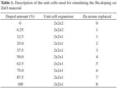
COMPUTATIONAL METHODOLOGY The simulation for ZnO material was performed based on a wurtzite structure in accordance to Özgür and co-workers.23 A Ba-doped model (Ba:ZnO) was developed from unit cell expansion in the direction of axes a, b and c, resulting at 12.5-100% doping (Figure 1 and Table 1). For all models, the TZVP44 basis set was employed to describe the Zn and O atoms; whereas, the Ba atoms were described by Zagorac45 basis set employing the HAYWSC46 pseudopotential.
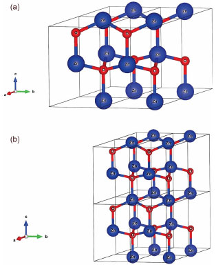 Figure 1. Crystalline structures for Ba:ZnO materials. a) 2x2x1 wurtzite supercell. b) 2x2x2 wurtzite supercell
The calculation level applied was based on the Density Functional Theory (DFT) at set B3LYP hybrid functional;47-50 SCF convergence was truncated in 10-8 Hartree and Mohnkhost-Pach51,52 method defined as 8x8 using CRYSTAL0953,54 software. Vibrational calculations were also performed using the optimized results for all models to evaluation of thermodynamic stability at room temperature (298.5 K) and 1 atm. The theoretical results discussed were Density of States (DOS) Projections and Band Structure analysis. The XCrysden55,56 Software was used for the structural analysis. Ubuntu Linux platforms made up by seven quad-core AMD computers with 32 GB of RAM and data storage capability of 3.5 TB were used in all simulations.
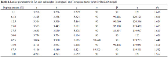
RESULTS AND DISCUSSION Zn(1-x)BaxO Structural Properties In 1921, Lars Vegard investigated the amount of doping effect on the crystalline structure of ionic structures through X-Ray diffraction (XRD) showing an empirical rule, which was called "Vegard's Law". This rule is a linear relationship between lattice parameters and impurity amount and it was improved by Barret (1952), Hume-Rothery and partners (1969) and Benett (1979); furthermore, studies have shown that the crystalline structure is influenced by atomic size, volume and number of electron ratio, the doping effects on the Brillouin Zone and the electrochemical differences between the elements. According to Vegard's law, the linear behaviour is associated to the doping process, which causes lattice parameters reduction and exhibits an attractive character between atoms. On the other hand, the nonlinear increase in lattice parameters presents a repulsive character between atoms. Therefore, an ideal behaviour for a solid solution is characterized by a linear increase in lattice parameters regarding the doping amount in a crystalline structure, indicating the possibility of synthesis.57,58 Theoretical results for ZnO lattice parameters and band-gap are shown in the Table 1S in Supplementary Material (SM). It is observed that lattice parameters are in good agreement with X-Ray Diffraction and other theoretical results; whereas, the band gap is in accordance with the expected value of 3.37 eV.13-15,25,26 Structural results for Ba:ZnO models (Table 2) are discussed through lattice parameters. For wurtzite structure, a= b ≠ c lattice parameters and α = β = 90º and γ = 120º angles; however, the Ba-doping at 6.25%, 12.5%, 25%, 37.5%, 62.5%, 75% and 87.5% shows a crystalline phase distortion, once the a and b lattice parameters and β and γ angles presented deviation from the expected values for a wurtzite structure. Nevertheless, the Brillouin Zone and tetragonality factor (c/a) were slight modified after the doping process keeping wurtzite-ZnO structure. The lattice parameters variation is caused by bond length increase after the doping process. In the ZnO material, the Zn - O bond length is 1.980 Å; whereas, in the Ba-doped models there is a tetrahedron distortion evidenced by deviation in the Zn - O bond lengths. In particular, the Ba-doped models from 6.25% to 37.5%, the Zn - O and Ba - O bond lengths were 1.941 Å and 2.016 Å, respectively; whereas, for percentages from 62.5% to 87.5%, such bond lengths were calculated between 2.003 Å and 2.203 Å, respectively. For Ba-doped models at 50% and 100%, the Zn-O and Ba-O bond lengths were calculated at 1.980 Å and 2.497 Å, respectively. For the doped model at 62.5%, c lattice parameter is not linearly affected by Ba atoms insertion in crystalline structure. Such deviation from wurtzite-ZnO crystalline structure was caused because of unequal distribution of the Ba atoms amount in relation to tetrahedron sites number; consequently, the Ba atoms in excess are concentred in a region along of ZnO unit cell as consequence of random distribution in the occupation of tetrahedron sites. Although, the wurtzite crystalline phase distortion occurs, there is a linear increase of lattice parameters in relation to Ba-doping in according to Vegard's law. Thus, the Ba atoms insertion in the wurtzite-ZnO structure can be characterized as an ideal behaviour indicating the possible formation of solid solution. In Thermodynamic Stability Evaluation Section, we present an theoretical investigation from Gibbs Free Energy stability for Ba:ZnO materials.
Electronic Property The electronic properties of ZnO and Ba:ZnO materials were evaluated through the projected Density of States (DOS), Figure 1S. Such DOS results are evaluated from last five energy bands of the Valence Band (VB) and first five energy bands of the Conduction Band (CB) featuring the band-gap region (Eg). In the ZnO model, the O atoms largely contributed to composition on all VB and for higher energy levels of CB. The VB energy levels were predominantly made for 2p orbitals; whereas, the CB energy levels were composed of 2p and 3s orbitals. Zn atoms showed low contribution by 3d and 4s orbitals at the top of VB; whereas, doping process shows low impact on the O and Zn orbitals contributions in VB and CB. Barium atoms were predominant at the top of the VB through 5p orbitals in large proportion; while, 3d orbitals were calculated as low contribution. Regarding CB, the Ba atoms contribution was calculated mainly through 3d and 5s orbitals. The insertion of Ba atoms shows a strong effect on the energy of the top of the VB and bottom of CB as better discussed on Optical Properties Section. Besides, doping process also reduces the contribution of the oxygen atom on CB causing modification of Eg. Such modification is based on change in the VB and CB energy levels; for Eg of ZnO material the energy levels for top of VB and bottom of CB are observed from -10 to -6 eV and -2 to 11 eV, respectively; whereas, for doped materials such bands are calculated from -6 to -5 eV and -2 to 2 eV, respectively. Then, from same number of energy levels analyzed was noted an energetic equiparation of these electronic levels or an electronic degeneration (see SM - Figure 1S and Figure 2S). Optical Property The optical property of a solid is defined as an interaction between the solid and electromagnetic radiation. Semiconductor materials interact only with electromagnetic energy equal to or higher than Eg.59,60 Therefore, the presence of Ba atoms in the crystalline structure causes changes in the band structure (Figure 2S); mainly, through variation in Eg calculated to 6.12%, 12.5%, 25%, 37.5%, 50% and 100% models, all with indirect Eg (Figure 2S). On the other hand, the direct Eg (Figure 2S) calculated to 0%, 62.5%, 75% and 87.5% models show wavelengths associated from Middle Ultraviolet to Ultraviolet-Visible (UV-Vis), Table 2S in SM. We evaluate the optical property through Eg values (Table 2S - SM) showing that a non-linear Eg plot in relation to Ba doping. To discuss such non-linear behaviour of Eg, all results for Ba:ZnO (Egmodel) were referenced to the ZnO material (Egpure) as shown in Equation 1 and plotted in Figure 2. 
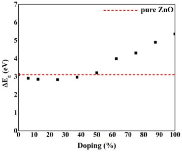 Figure 2. Theoretical results in according to ZnO band gap to Ba-dopant amount
According to Figure 2, only the doped models from 6.35% to 37.5% have satisfactory results for Eg decrease in relation to ZnO. For the Ba-doped models above 50%, the results show the increase of Eg. To visualize better such changes (ΔEg - Figure 3), the top of VB and bottom of CB energy levels were referenced to ZnO (Figure 3). These results indicate an increase between 2.2 eV and 4.4 eV in energy at the top of VB and bottom of CB, respectively. Therefore, the energy presented by 6s, 6p and 3d atomic orbitals in doped materials were higher than ZnO (see SM, Figure 1S).
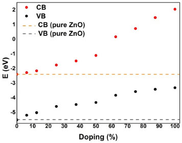 Figure 3. Energy levels calculated from DFT/B3LYP at the top of Valence Band (VB) and the bottom of Conduction Band (CB) according to Ba-doping amount and referenced to ZnO
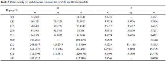
Ferroelectric Property In a ferroelectric material, the direction of charge polarization can be reversed by applying an external electrical field, which is very important to the charge storage property. In order to better understand such property, the solid state theory developed the dielectric constants (ε) and polarizability (α) concepts. In general, the dielectric constant determines the charge storage capacity; whereas, the polarizability describes how much a material is polarizable under an electrical field. Once these values increase, the material has a high ferroelectric property; however, as ε as α are dependents on the tensor matrix, which is directed similarly to Cartesian coordinates system.59 The ε and α results for ZnO and Ba:ZnO models are presented in the Table 3. It is observed that the doping process improves the dielectric constants for Ba-doped models from 6.12% to 87.5% because theoretically there is an increase in all tensor matrix components in relation to ZnO. The highest value for dielectric constant was simulated for Ba-doped model at 87.5%. Regarding doping at 100%, a decrease in ε for three components in relation to ZnO was observed.
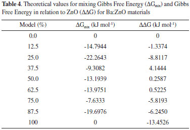
The increase observed in the ε and α results in relation to Ba-doping can be understood due to the tetrahedron distortion in the wurtzite structure. Such distortions are evidenced by changes in the bond length after the doping process (see Structure Properties Section) and they are responsible for the increase of the dielectric constants and polarizability. Another point is associated to the atoms which were distributed randomly in crystalline structure causing a symmetry lower than ZnO; consequently, the electronic density was disorderly distributed and provided ferroelectric and dielectric properties higher than those in the ZnO. Recently, the perovskite-type materials have been largely employed in the development of ferroelectric memories and charge storage devices because they present high values for polarizability and dielectric constants.13-18 However, the production process of such devices is hampered due to the difficulty of interface between perovskite-type structure and Si substrate.13,19-21 ZnO and Ba-doped ZnO can be easily adjusted to this substrate because of similar structures; such as, tetrahedral sites, hexagonal group and lattice parameters. Based on our theoretical results, the ZnO:Ba at 87.5% is a potential alternative to replace perovskite-type materials in ferroelectric devices, for instance, Random Access Memory (RAM), flash-type memories or flash-drives; nevertheless, the structural instability forecasted can be a great challenge to synthesis methods. Thermodynamic Stability Evaluation Structure properties results indicated that the Ba:ZnO materials have showed an ideal character according to Vegard's law. Thus, it is expected that such materials can be obtained by experimental techniques, once the crystalline structure are linearly changed with the dopant amount. However, in literature some manuscripts focused on Ba:ZnO materials29,35,61-64 report that the solubility of Ba atoms is limited at 5% mol in wurtzite-ZnO structure. These manuscripts also present temperature influence on Ba solubility, which is slightly increased in high temperatures. Nevertheless, such Ba solubility decrease with the temperatures reduction and there is segregation of Ba atoms inside wurtzite-ZnO structure. Assuming that the Vegard's law prevision is not enough to determines the stability of Ba:ZnO materials. Therefore, from vibrational calculations based on DFT/B3LYP we calculate the mixing Gibbs Free Energy (ΔGmix - Eq. 2) and Gibbs Free Energy in relation to pure ZnO (ΔΔG - Eq. 3).   The positive value for ΔΔG of these models indicates that these models are not favorable to be obtained through experimental techniques. Then, the obtained results for Thermodynamic Stability of Ba-doped and pure ZnO (Table 4) show instability for 37.5%, 50% and 62.5% doping at room conditions from positive ΔΔG values calculated, whereas; 12.5%, 25.0%, 75% and 87% doping indicate a stability at room conditions. For many years, experimental techniques showed a Ba solubility in the ZnO structure limited at 2.5% mol, such techniques were based on traditional techniques, such as, precipitation and ceramic simple synthesis.35,61-63 Nowadays, Srinet and coauthors29 employed a thermal decomposition method increasing the Ba solubility to 5% mol at ZnO structure in accordance with theoretical results presented on Table, which indicate that the Ba-doped models from low amount, 6.25%, 12.5% and 25%, show negative values for ΔΔG and are stables at room temperature. Thus, the Ba solubility limit can be estimate as 25% in relation to Zn amount from modern experimental techniques. For 37.5%, 50% and 62.5% doping, we propose that these structures are unstable at room conditions due to a spinodal behavior, which is a region of phase diagram where simple oxides are more stables than solid solution.65 Examples for spinodal behavior in solid solutions are TiO2-SnO2,66-68 TiO2-VO269 and ZnO-CdO70 compounds.
CONCLUSION We used DFT with periodic model to discuss structure, electronic, optical and ferroelectric properties available for Ba doping in ZnO. Electronic and optical properties showed that Ba-doping from 6.12% to 37.5% are potential alternatives to be employed in electronic and optical devices, once the band-gap decrease changes the profile wavelength to the visible range. For Ba-doped model at 50% was calculated a band-gap very close to pure ZnO; while the Ba-doped models above 62.5% have insulating character. The band-gap variation is caused by Ba atoms influencing as Valence Band as Conduction Band. The ferroelectric property was evaluated for all models and presented Ba-doping as a good alternative to improve the ferroelectric properties of ZnO materials. However, the thermodynamic stability indicates that Ba solubility in ZnO-wurtzite structure is limited at 25% regarding to Zn position in unit cell. Thus, the Ba:ZnO models below 25% can be obtained through experimental techniques. Therefore, the Ba-doped ZnO materials have showed as potential alternatives to replace perovskite-type in ferroelectric devices employed in several electronic and optical devices, solar cells, and photocatalytic processes.
ACKNOWLEDGMENTS The authors acknowledge support from CNPq, CAPES and Fundação Araucária.
SUPPLEMENTARY MATERIAL The Tables 1S and 2S as well as the Projected Density of States (Figure 1S) and Band Structures (Figure 2S) are available at http://www.quimicanova.sbq.org.br in PDF format with free access.
REFERENCES 1. Chew, Z. J.; Li, L.; Mater. Lett. 2013, 91, 298. DOI: http://dx.doi.org/10.1016/j.matlet.2012.10.011 2. Xun, C.; Xiaomin, L.; Xiangdong, G.; Xinjun, L.; Chang, Y.; Rui, Y.; Ping, J.; J. Phys. D: Appl. Phys. 2011, 44, 255104. DOI: http://dx.doi.org/10.1088/0022-3727/44/25/255104 3. Gupta, M. K.; Sinha, N.; Kumar, B.; J. Appl. Phys. 2012, 112, 014303. DOI: http://dx.doi.org/10.1063/1.4730933 4. Zhang, F.; Li, X.; Gao, X.; Wu, L.; Zhuge, F.; Wang, Q.; Liu, X.; Yang, R.; He, Y.; Solid State Commun. 2012, 152, 1630. DOI: http://dx.doi.org/10.1016/j.ssc.2012.04.073 5. Nedic, S.; Tea Chun, Y.; Hong, W.-K.; Chu, D.; Welland, M.; Appl. Phys. Lett. 2014, 104, 033101. DOI: http://dx.doi.org/10.1063/1.4862666 6. Gupta, M. K.; Kumar, B.; J. Mater. Chem. 2011, 21, 14559. DOI: http://dx.doi.org/10.1039/c1jm12107c 7. Qiuhong, T.; Jinbin, W.; Xiangli, Z.; Yichun, Z.; Qianjin, W.; Yi, Z.; Zhang, X.;Huang, S.; IEEE Trans. Electron Devices 2011, 58, 2738. DOI: http://dx.doi.org/10.1109/TED.2011.2157348 8. Sohn, J. I.; Choi, S. S.; Morris, S. M.; Bendall, J. S.; Coles, H. J.; Hong, W.-K.; Jo, G.; Lee, T.; Welland, M. E.; Nano Lett. 2010, 10, 4316. DOI: http://dx.doi.org/10.1021/nl1013713 PMID: 20945844 9. Lee, S.; Kim, H.; Yun, D.-J.; Rhee, S.-W.; Yong, K.; Appl. Phys. Lett. 2009, 95, 262113. DOI: http://dx.doi.org/10.1063/1.3173817 10. Lee, D. U.; Kim, E. K.; Cho, W.-J.; Kim, Y.-H.; Im, H.; Thin Solid Films 2012, 521, 98. DOI: http://dx.doi.org/10.1016/j.tsf.2012.02.044 11. Zhao, J.-W.; Liu, F.-J.; Huang, H.-Q.; Hu, Z.-F.; Zhang, X.-Q.; Chin. Phys. B 2012, 21, 065201. DOI: http://dx.doi.org/10.1088/1674-1056/21/6/065201 12. Kang, Y. H.; Choi, J.-H.; Lee, T. I.; Lee, W.; Myoung, J.-M.; Solid State Commun. 2011, 151, 1739. DOI: http://dx.doi.org/10.1016/j.ssc.2011.08.036 13. Wang, W.; Zhao, Q.; Xu, J.; Yu, D.; CrystEngComm 2012, 14, 3015. DOI: http://dx.doi.org/10.1039/C1CE05810J 14. Cho, S.; Kim, S.; Oh, E.; Jung, S.-H.; Lee, K.-H.; CrystEngComm 2009, 11, 1650. DOI: http://dx.doi.org/10.1039/b902130b 15. Chen, P.; Gu, L.; Cao, X.; CrystEngComm 2010, 12, 3950. DOI: http://dx.doi.org/10.1039/c001615b 16. Yang, Y.; Qi, J.; Guo, W.; Liao, Q.; Zhang, Y.; CrystEngComm 2010, 12, 2005. DOI: http://dx.doi.org/10.1039/b927165a 17. Brillson, L. J.; Lu, Y.; J. Appl. Phys. 2011, 109, 121301. DOI: http://dx.doi.org/10.1063/1.3581173 18. Lee, Y.; Lee, S.; Ryu, H. T.; Kim, D. Y.; AIP Conf. Proc. 2011, 1399, 163. 19. Glinchuk, M. D.; Kirichenko, E. V.; Stephanovich, V. A.; Zaulychny, B. Y.; J. Appl. Phys. 2009, 105, 104101. DOI: http://dx.doi.org/10.1063/1.3126507 20. Lee, Y.; Kim, D.; Lee, S.; Fu, D.; J. Korean Phys. Soc. 2012, 60, 1891. DOI: http://dx.doi.org/10.3938/jkps.60.129 21. Dhananjay, Nagaraju, J.; Krupanidhi, S. B.; J. Appl. Phys. 2007, 101, 104104. DOI: http://dx.doi.org/10.1063/1.2722243 22. Singh, D. P.; Gupta, S. K.; Srivastava, A.; Manohar, R.; J. Lumin. 2013, 139, 60. DOI: http://dx.doi.org/10.1016/j.jlumin.2013.02.037 23. Özgür, Ü.; Hofstetter, D.; Morkoc, H.; Proc. IEEE 2010, 98, 1255. DOI: http://dx.doi.org/10.1109/JPROC.2010.2044550 24. Özgür, Ü.; Alivov, Y. I.; Liu, C.; Teke, A.; Reshchikov, M. A.; Doğan, S.; Avrutin, V.; Cho, S.-J.; Morkoç, H.; J. Appl. Phys. 2005, 98, 041301. DOI: http://dx.doi.org/10.1063/1.1992666 25. Klingshirn, C.; ChemPhysChem 2007, 8, 782. DOI: http://dx.doi.org/10.1002/cphc.200700002 PMID: 17429819 26. Shen, X.; Sun, J.; Zhu, G.; Ji, Z.; Chen, Z.; Li, N.; J. Mater. Sci. 2013, 48, 2358. DOI: http://dx.doi.org/10.1007/s10853-012-7017-7 27. West, A. R.; Basic solid state chemistry, 2th ed., John Wiley & Sons: Chichester, 2006. 28. Marana, N. L.; Sambrano, J. R.; de Souza, A. R.; Quim. Nova 2010, 33, 810. DOI: http://dx.doi.org/10.1590/S0100-40422010000400009 29. Srinet, G.; Kumar, R.; Sajal, V.; Mater. Lett. 2014, 126, 274. DOI: http://dx.doi.org/10.1016/j.matlet.2014.04.054 30. Lee, S.; Lee, Y.; Young Kim, D.; Won Kang, T.; J. Appl. Phys. 2013, 114, 064102. DOI: http://dx.doi.org/10.1063/1.4817765 31. Schubert, M.; Ashkenov, N.; Hofmann, T.; Lorenz, M.; Hochmuth, H.; v. Wenckstern, H.; Grundmann, M.; Wagner, G.; Ann. Phys. 2004, 13, 61. DOI: http://dx.doi.org/10.1002/andp.200310047 32. Voora, V. M.; Hofmann, T.; Schubert, M.; Brandt, M.; Lorenz, M.; Grundmann, M.; Ashkenov, N.; Schubert, M.; Appl. Phys. Lett. 2009, 94, 142904. DOI: http://dx.doi.org/10.1063/1.3116122 33. Voora, V. M.; Hofmann, T.; Brandt, M.; Lorenz, M.; Ashkenov, N.; Grundmann, M.; Schubert, M.; Appl. Phys. Lett. 2009, 95, 082902. DOI: http://dx.doi.org/10.1063/1.3211914 34. Böntgen, T.; Schöche, S.; Schmidt-Grund, R.; Sturm, C.; Brandt, M.; Hochmuth, H.; Lorenz, M.; Grundmann, M.; Thin Solid Films 2011, 519, 2933. DOI: http://dx.doi.org/10.1016/j.tsf.2010.12.064 35. Fan, J.;Freer, R.; J. Mater. Sci. 1997, 32, 415. DOI: http://dx.doi.org/10.1023/A:1018561602083 36. Jindal, K.; Tomar, M.; Katiyar, R. S.; Gupta, V.; J. Appl. Phys. 2012, 111, 102805. DOI: http://dx.doi.org/10.1063/1.4714686 37. Sun, J.; Bian, J.; Wang, Y.; Zhang, S.; Wang, Y.; Feng, Q.; Liang, H.; Du, G.; Thin Solid Films 2012, 521, 253. DOI: http://dx.doi.org/10.1016/j.tsf.2011.10.202 38. Dutta, R.; Mandal, N.; Appl. Phys. Lett. 2012, 101, 042106. DOI: http://dx.doi.org/10.1063/1.4738990 39. Bantounas, I.; Goumri-Said, S.; Benali Kanoun, M.; Manchon, A.; Roqan, I.; Schwingenschlögl, U.; J. Appl. Phys. 2011, 109, 083929. DOI: http://dx.doi.org/10.1063/1.3574924 40. Otal, E. H.; Yoon, S.; Aguirre, M.;Weidenkaff, A.; J. Alloys Compd. 2011, 509, Supplement 1, S364. DOI: http://dx.doi.org/10.1016/j.jallcom.2011.02.076 41. Hwan Ko, Y.; Hyun Lee, S.; Su Yu, J.; Appl. Phys. Lett. 2013, 103, 022911. DOI: http://dx.doi.org/10.1063/1.4813543 42. Yang, Y. C.; Song, C.; Wang, X. H.; Zeng, F.; Pan, F.; Appl. Phys. Lett. 2008, 92, 012907. DOI: http://dx.doi.org/10.1063/1.2830663 43. Heo, S.; Sharma, S. K.; Lee, S.; Lee, Y.; Kim, C.; Lee, B.; Lee, H.; Kim, D. Y.; Thin Solid Films 2014, 558, 27. DOI: http://dx.doi.org/10.1016/j.tsf.2014.02.025 44. Peintinger, M. F.; Oliveira, D. V.; Bredow, T.; J. Comput. Chem. 2013, 34, 451. DOI: http://dx.doi.org/10.1002/jcc.23153 PMID: 23115105 45. Zagorac, D.; Doll, K.; Schön, J. C.; Jansen, M.; Chem. - Eur. J. 2012, 18, 10929. DOI: http://dx.doi.org/10.1002/chem.201200180 46. Hay, P. J.;Wadt, W. R.; J. Chem. Phys. 1985, 82, 299. DOI: http://dx.doi.org/10.1063/1.448975 47. Stephens, P. J.; Devlin, F. J.; Chabalowski, C. F.; Frisch, M. J.; J. Phys. Chem. 1994, 98, 11623. DOI: http://dx.doi.org/10.1021/j100096a001 48. Becke, A. D.; J. Chem. Phys. 1993, 98, 5648. DOI: http://dx.doi.org/10.1063/1.464913 49. Becke, A. D.; Phys. Rev. A 1988, 38, 3098. DOI: http://dx.doi.org/10.1103/PhysRevA.38.3098 50. Lee, C.; Yang, W.; Parr, R. G.; Phys. Rev. B 1988, 37, 785. DOI: http://dx.doi.org/10.1103/PhysRevB.37.131 51. Monkhorst, H. J.; Pack, J. D.; Phys. Rev. B 1976, 13, 5188. DOI: http://dx.doi.org/10.1103/PhysRevB.13.5188 52. Pisani, C.; Dovesi, R.; Roetti, C.; Hartree-Fock ab initio Treatment of Crystalline Systems.; Springer Berlin Heidelberg: 1988. 53. Dovesi, R.; Orlando, R.; Civalleri, B.; Roetti, C.; Saunders, V. R.; Zicovich-Wilson, C.-M.; Zeitschrift für Kristallographie 2005, 220, 571. 54. Dovesi, R.; Saunders, V. R.; Roetti, C.; Orlando, R.; Zicovich-Wilson, C. M.; Pascale, F.; Civalleri, B.; Doll, K.; Harrison, N. M.; Bush, I. J.; D'Arco, P.; Llunell, M.; CRYSTAL09 User's Manual, University of Torino: Torino, 2009. 55. Kokalj, A.; J. Mol. Graphics Modell. 1999, 17, 176. DOI: http://dx.doi.org/10.1016/S1093-3263(99)00028-5 56. Kokalj, A.; Comput. Mater. Sci. 2003, 28, 155. DOI: http://dx.doi.org/10.1016/S0927-0256(03)00104-6 57. Denton, A. R.; Ashcroft, N. W.; Phys. Rev. A 1991, 43, 3161. DOI: http://dx.doi.org/10.1103/PhysRevA.43.3161 PMID: 9905387 58. Vegard, L.; Z. Physik 1921, 5, 17. DOI: http://dx.doi.org/10.1007/BF01349680 59. Smart, L. E.; Solid state chemistry: an introduction, 3th ed., Taylor & Francis: Boca Raton, 2005. 60. Kwok, H. L.; Electronic Materials, PWS Publishing Company: Boston, 1997. 61. Uematsu, K.; Morimoto, T.; Kato, Z.; Uchida, N.; Sa'to, K.; J. Mater. Sci. Lett. 1987, 6, 1285. DOI: http://dx.doi.org/10.1007/BF01794591 62. Ghashang, M.; Rajabi, A. R.; Jabbarzare, S.; Shafiee, M. R. M.; Curr. Nanosci. 2014, 10, 312. DOI: http://dx.doi.org/10.2174/157341371130900101 63. Water, W.; Fang, T.-H.; Ji, L.-W.; Meen, T.-H.; Yan, Y.-S.; Journal of Science and Innovation 2011, 1, 25 64. Lare, Y.; N'Konou, K.; Haris, M.; Baneto, M.; Amou, K. A.; Napo, K.; Adv. Mater. 2014, 3, 63. DOI: http://dx.doi.org/10.11648/j.am.20140306.11 65. Zakrzewska, K.; Thin Solid Films 2001, 391, 229. DOI: http://dx.doi.org/10.1016/S0040-6090(01)00987-7 66. Padurow, N. N.; Naturwissenschaften 1956, 395. DOI: http://dx.doi.org/10.1007/BF00594009 67. Sensato, F. R.; Custodio, R.; Longo, E.; Beltrán, A.; Andrés, J.; Catal. Today 2003, 85, 145. DOI: http://dx.doi.org/10.1016/S0920-5861(03)00382-1 68. Cassia-Santos, M. R.; Souza, A. G.; Soledade, L. E. B.; Varela, J. A.; Longo, E.; J. Therm. Anal. Calorim. 2005, 79, 415. DOI: http://dx.doi.org/10.1007/s10973-005-0076-0 69. Hiroi, Z.; Yoshida, T.; Yamaura, J.; Okamoto, Y.; APL Mater. 2015, 3, 062508. DOI: http://dx.doi.org/10.1063/1.4919764 70. Lashkarev, G. V.; Shtepliuk, I. I.; Ievtushenko, A. I.; Khyzhun, O. Y.; Kartuzov, V. V.; Ovsiannikova, L. I.; Karpyna, V. A.; Myroniuk, D. V.; Khomyak, V. V.; Tkach, V. N.; Timofeeva, I. I.; Popovich, V. I.; Dranchuk, N. V.; Khranovskyy, V. D.; Demydiuk, P. V.; Low Temp. Phys. 2015, 41, 129. DOI: http://dx.doi.org/10.1063/1.4908204 |
On-line version ISSN 1678-7064 Printed version ISSN 0100-4042
Qu�mica Nova
Publica��es da Sociedade Brasileira de Qu�mica
Caixa Postal: 26037
05513-970 S�o Paulo - SP
Tel/Fax: +55.11.3032.2299/+55.11.3814.3602
Free access


