Nota Técnica
| Superhydrophobic silicon fabricated by phosphomolybdic acid-assisted electrochemical etching |
|
Yanbiao Zhou*; Kaige Qu; Lihui Zhang; Binghua Liao
School of Chemistry and Environmental Engineering, Pingdingshan University, Pingdingshan 67000, China Recebido em 11/02/2019 *e-mail: 349633279@qq.com Controllable geometry silicon surfaces with superhydrophobicity are difficult to be fabricated without photolithography techniques. Superhydrophobic silicon surfaces with water contact angle larger than 150° and sliding angle less than 10° have been successfully fabricated by electrochemical etching strategy. Squarelike hole arrays with controllable geometries, especially ole width and depth were formed on silicon. Compared with the chemical composition, the obvious change of the hole size and surface roughness with etching time was actually the intrinsic factors for wetting regulation. The superhydrophobic silicon exhibited good stability even after storage in air and oil for 2 months. Moreover, the relatively stable superhydrophobic silicon exhibited good self-cleaning and water-proofing properties in air and oil. INTRODUCTION Superhydrophobic surface possesses self-cleaning and waterproof abilities, leading to the removal of water and contaminants from optoelectronic device surface, such as solar cells and chip microfluidic devices.1-3 For the practical applications of superhydrophobic silicon devices, superhydrophobicity control of silicon surface has been considered to be an important issue to study in surface engineering.4-6 Typically silicon superhydrophobicity is achieved by separately constructing multiscale topography, followed by coating it with low surface energy materials, such as silicon-containing and fluorine-containing substances. However, silicon may lose superhydrophobicity due to the detachment and decomposition of coating in practical applications.7,8 Furthermore, the properties such as conductivity of the silicon probably get weaken or lost after surface coating. By contrast, the etching strategy can overcome such problems.9 By way of etching, the surface structures have the same phase as the substrate does. Such surfaces are considered to have more potential applications in modern technology.10,11 Uniform structures of silicon surface are usually fabricated by utilizing various experimental setups and chemical formulas.12,13 Nevertheless, the fabrication of superhydrophobic silicon surfaces with new uniform geometric structures without surface modification and photolithography technique is still a challenge.14 Especially, multihole silicon structures exhibit superhydrophobicity without coatings has rarely been established.15 Such superhydrophobic silicon surface is typically achieved by fabricating hierarchical micro/nano dual-scale structures via laser, reactive ion, wet or electrochemical etching surface approaches.7,14-16 However, either superhydrophobic stability was not studied or it was reported to be inadequate. In this study, superhydrophobic silicon with controllable geometries, i.e., controllable width and depth square-like holes, was fabricated by phosphomolybdic acid-assisted electrochemical etching. Importantly, coating and photolithography were not needed for silicon superhydrophobicity.17 The superhydrophobic silicon exhibited good stability almost without significantly losing superhydrophobicity even after placement in air and oil for 2 months. The superhydrophobicity may probably be useful in the application of self-cleaning squarelike hole devices.
EXPERIMENTAL Materials Silicon wafers (3-15 Ω·cm resistivity) were provided by Lijing Silicon Material. (Zhejiang, China). Phosphomolybdic acid (PMA) was obtained from Alfa Aesar GmbH (Karlsruhe, Germany). Hydrofluoric acid (HF), hydrogen peroxide (H2O2) and absolute ethanol were supplied by Fuchen Chemical Industries (Tianjin, China). All other chemicals were analytical grade reagents and used without further purification. Silicon electrolysis process Polished n-type and p-type (100) silicon wafers with 525 μm thick were cut into 1×5 cm2 slices as substrates. Prior to electrochemical etching, they were dipped in 10% hydrogen fluoride solution for 5 min to remove silicon-dioxide layer. The electrolytic solution of the electrochemical etching process consisted 60 mL absolute ethanol, 40 mL HF (40% Hydrofluoric acid), 7.5 mL H2O2 (30% hydrogen peroxide) and 0.4 mL PMA ethanol solution (10-2 mol L-1). The silicon slice as an anode and a graphite rod as a cathode were connected to positive and negative poles of a direct current (DC) power supply (PS-303DM, Longwei Instrument), respectively. Both graphite rod and silicon slice were placed into the electrolytic solution which was contained in a single-tank cell, and a constant current intensity 30-40 mA cm-2 was applied between them. The area of the polished silicon slice exposed to electrolytic solution was fixed at 1 cm2 for all the experiments. The whole process was carried out in a room-temperature environment without temperature control during a temperature variation of the electrolytic solution from 20 to 36 °C. After electrochemically etched for a certain time, the resulting silicon was rinsed by ethanol and then dried at room temperature. It should be noted that the HF solution is dangerous and must be handled under a well-ventilated fume hood with great care while wearing appropriate chemical safety protection. Instruments and characterization The contact angles the as-prepared surface were measured by a Attension Theta System (PD-200, Sweden) under ambient conditions with approximately 4 µL distilled water or oil droplet. Their corresponding sliding angles were determined using a tilting stage and the sample stage was tilted until droplet started to move. Each sample was measured 3 times at different positions and the average value was used as the final result. The surface morphology of the obtained samples was investigated using field emission scanning electron microscopy (FESEM, Hitachi SU8000, Japan). The chemical composition of the as-prepared surface was analyzed by an energy-dispersive analyzer. Fourier transform infrared (FTIR)-attenuated total reflection (ATR) spectra in the wavenumber range of 4000-600 cm-1 were recorded on a Brucker Tensor 37 spectrometer (Bruker Optics, Germany) equipped with a MIRacle ATR accessory (Pike technologies, USA). The roughness (Ra) of the multihole silicon was determined by a white light interferometer (Contour GT-K, Bruker, USA).
RESULTS AND DISCUSSION Surface morphologies FESEM was used to examine the typical top and side morphology of the silicon surface etched for different time. Figures 1 and 2 present the top and side SEM images of the silicon surface at low and high magnifications for different etching time, where a uniform square-like hole array is patterned on the silicon surface. The formation of inhomogeneous square-like holes is probably ascribed to HF–2 ion anisotropy and silicon crystal orientation.18,19 That is to say, the shape of holes formed may depend on the interaction HF–2 anisotropy with silicon orientation. Studies were also carried out using H2O2/HF or phosphomolybdic acid/HF solution as the etchant solution and keeping all other experimental conditions the same. Interestingly, gradient square-like holes were observed for less than 4 h etching time in H2O2/HF solution, while similar gradient square-like holes was formed for more than 4 h etching time in phosphomolybdic acid/HF solution. These results not only further confirmed the anisotropy etching of silicon by HF– 2, but also suggested that both H2O2 and phosphomolybdic acid can contribute to anisotropy etching of silicon, enabling the formation square-like holes in longer etching time range.
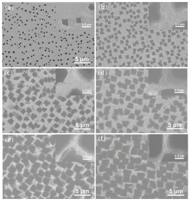 Figure 1. FESEM images of the top views of silicon surfaces with different etching time: (a) 20 min, (b) 40 min, (c) 1 h, (d) 3 h, (e) 5 h, (f) 7 h. Insets are the corresponding high magnification images
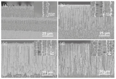 Figure 2. FESEM images of the side views of silicon surface under different etching time: (a) 20 min, (b) 40 min, (c) 4 h, (d) 7 h. Insets are the corresponding high magnification images
The images were statistically analyzed using ImageJ® software for calculating average hole width, depth and porosity. These holes were parallel to each other and their widths were found to be quite constant with increasing hole depth. When etching time was changed from 20 min to 7 h, the calculated average hole width, depth and porosity were increased from 0.2 µm to 3.0 µm, 10 µm to 90 µm and 9.7% to 71.7%, respectively. This means that when the etching time was gradually increased, the surface porosity correspondingly increased. The enlarged views of the surface of the etched silicon are illustrated in Figure 1. Obviously, finer structures on the silicon surface were observed, which further improved the surface roughness of silicon. This hierarchical structure of the etched silicon surface contributed significantly to the formation of superhydrophobicity. Chemical composition In addition to the surface structure, the chemical composition of multihole surface is another important factor for determining the surface wettability. A great deal of silicon-bonded hydrogen was formed during the formation of holes when silicon was etched in the HF-containing electrolytic solution.20,21 The synergistic effect of multihole surface and chemical composition imparted hydrophobic properties. However, after electrochemical etching, the longer silicon stored in air, the more hydroxyl groups formed on the surface.22 This change of surface chemical composition will lead to the decrease of water contact angle. Thus, the electron diffraction spectroscopy (EDS) analysis of the etched silicon with increasing electrolysis time was performed by energy dispersive spectrometer. EDS spectra are acquired to investigate the element composition of the hole border after anodic etching (Table 1). The element composition given in Table 1 is a mean atomic percentage. Interestingly, the percentage of hydrophilic oxygen on the etched silicon surface progressively decreased from 7.5% to 0% with increasing etching time, whereas the atomic percentage of hydrophobic silicon increased from 92.5% to 100%. As shown in Figure 3a, only peaks of Si and O are detected on the silicon etched for 1 h. When the etching time is 7 h, the etched silicon surface is composed of almost entirely of silicon. This variation of surface chemical composition with etching time is in favour of the fabrication superhydrophobicity. The reason may be that more hydrogen was incorporated in micro-facet, resulting in the increase of hydrophobic dihydride and trihydride, and the corresponding decrease of hydrophilic hydroxyl and siloxy.
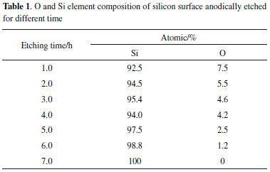
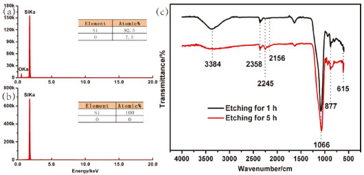 Figure 3. Element composition of the etched silicon. EDS spectra of the silicons etched for (a) 1 h and (b) 7 h after storage for 2 months in air, respectively. (c) FTIR transmittance spectra of the silicon etched for 1 h and 5 h after storage for 2 months in air
The influence of etching on the surface chemical composition of the multihole surface was further investigated by ATR-FTIR spectra. Figure 3 shows the FTIR transmission spectra measured from the silicon etched for 1 h and 5 h after storage for 2 months under ambient conditions. Compared with the sample etched for less time, an increase in the relative intensity of peaks at 2156, 2245 and 2358 cm-1 corresponding to the Si–Hx (x=1, 2, 3) (monohydride, dihydride and trihydride) stretching and bending vibration, and a decrease in the relative intensity of peaks at 877 and 1066 cm-1 corresponding to Si–O–Si bending and stretching vibrations is observed.23,24 Therefore, the results of the FTIR measurements reveal that electrolytic process enhances the hydrophobic hydrogen incorporation into the multihole silicon surface, resulting in the improvement of the hydrophobicity of silicon. Surface wettability The wettability change of the silicon surface was evaluated by contact angle and sliding angle. As shown in Figure 4, the original smooth silicon surface without etching exhibits hydrophilic property (water contact angle = 87°), which can be ascribed to the flat surface and hydrophilic hydroxyl groups. However, after electrolytic etching for 20 min, hydrophilic surface was transferred to the hydrophobic surface with the water contact angle of 117° successfully. As the etching time extended, water contact angle continuously increased. For the etching time in the range of 0-60 min, water contact angle was increasing sharply. When the etching time exceeded 1 h, surface superhydrophobicity tended to be stable, indicating the superhydrophobic nature of these surfaces. The change trend of water contact angle on the etched silicon was consistent with that of surface porosity and chemical composition. Specifically, the water contact angle increased with the increasing porosity and silicon-bonded hydrogen. Additionally, the etched silicon surfaces showed superoleophilic and underoil superhydrophobic properties.
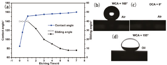 Figure 4. The wettability of the silicon etched after 6 hours. (a) The average water contact angle and sliding angle variation with etching time. Hollow squares represent sliding angles greater than 32°. (b) Water and (c) oil contact angle images. (d) Underoil water contact angle image
The water sliding angle decreased with increasing etching time. Especially, the water sliding angle of the surface etched for 5-7 h was less than 10°. The low sliding angle implies that water droplet may be in a nonwetting Cassie-Baxter state on the silicon.25 For the etched silicon, a great deal of air is trapped in the holes of silicon surface, offering a strong repellence to water. A composite solid-liquid-air three phase interface regime is formed, which may be interpreted by the typical Cassie–Baxter equation:26  where θr denotes the water contact angle on the etched silicon surface, θp denotes the water contact angle on the polished silicon surface (87°) and f is the liquid–solid contact area fraction. Therefore, when f decreases for a larger surface roughness, the water contact angle increases. Surface roughness of the multihole silicon is measured with white light interferometer and the obtained Ra roughness is increased from 0.14 to 4.1 µm by etching from 20 min to 7 h. Surface roughness induces the decrease of the solid-liquid contact (f), giving rise to the increase of water contact angle of the multihole surface. Therefore, the greater the surface roughness produced, the larger the water contact angle formed on multihole silicon surface. Moreover, the adhesion was reduced by a small area of solid−liquid interaction, consequently preventing the penetration of water droplets into the microscale hole and thus providing the surface with superhydrophobic ability. Superhydrophobic stability The superhydrophobic stability of the silicon etched for 6 h was evaluated in air and oil. Freshly prepared silicon tending to be oxidized by oxygen in air and oil is well established.27,28 Consequently, the study of its air and oil resistance is necessary. It is known that the natural silicon oxidation accompanies the exposure of siliocn to air and oil. With the oxidation by chemical species from the atmosphere, more hydrophilic hydroxyl groups cover the silicon surface. Therefore, these changes of chemical composition can influence the hydrophobicity of silicon surface. The chemical stability of the etched silicon was evaluated by exposing the silicon to air and oil. Figure 5 shows that the water contact angle of the silicon surface etched for 6 h changes with storage time, where insets are the corresponding photos. No significant change in water contact angle of silicon surface in air and oil was observed with the increase of storage time. For example, the water contact angle of silicon surface etched after 6 h gradually declined from about 160° to about 154° after storage for 2 months in oil, which verified that it can be stable for a long time. The results demonstrated that the superhydrophobicity can be stable for a long time in both water and oil.
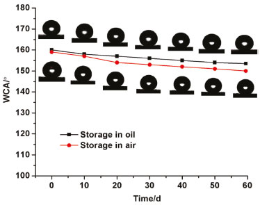 Figure 5. The water contact angle of the silicon surfaces etched for 6 h changes with storage time. The insets illustrate the images of water droplet on the corresponding surface
Self-cleaning and water-proofing properties Combining low water sliding angle and large water contact angle, the silicon exhibited self-cleaning properties. The silicon etched after 6 h was chosen to assess its dirt-removal properties with charcoal powder as artificial pollutant (with size in the range of 50–300 µm) in air. The etched surface is placed into a clear culture dish with a slight inclination angle of approximately 6° and initially randomly spread with charcoal powder (Figure 6a). When water droplet is continuously dropped on the etched surface, the pollutant is immediately picked up by the water-air interface of the rolling water droplet and carried away from the silicon surface on its rolling path (Figure 6b). No charcoal powder or water left on the area, indicating that the prepared silicon possessed good self-cleaning property (Video 1).
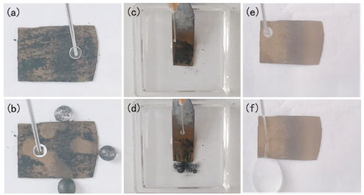 Figure 6. Self-cleaning and water-proofing abilities of the etched surface. Optical images of (a) the charcoal-contaminated surface in air, (b) the self-cleaned surface in air, (c) the charcoal-contaminated surface in oil, (d) the self-cleaned surface in oil and (e→f) the water proofing of the silicon surface etched for 6 h
Currently, self-cleaning effect of etched silicon with superhydrophobicity were usually investigated in air, not in oil.29 After wetted with oil, the change of physical and chemical properties of the surface usually leads to the weakening or even loss of the self-cleaning function. Hereby, the self-cleaning ability of the superhydrophobic and superoleophilic surface was evaluated in oil. For the etched silicon wetted by oil, the oil penetrates into holes and constructes a film of oil on the surface (Figure 6c). Because the surface energy of water is higher than that of oil, the water could not replace relatively stable oil film, showing underoil superhydrophobicity (Figure 4d). Accordingly, the formed slippery liquid-infused multihole surface can repel water droplets, resulting in that the charcoal powder can be easily washed off by the water droplets (Figure 6d and Video 2). The result suggested that the etched surface still remained its self-cleaning function in oily environments. The superhydrophobicity of the etched silicon also gave the etched surface excellent water-proofing property. Water proofing test of the silicon etched after 6 h was executed (Figure 6e and 6f). When water jet from a syringe was sprayed on the surface, it bounced off the silicon surface without leaving any water trace. This phenomenon indicated that the interaction between water and surface was weak (Video 3). The reason is that the etched silicon surface allows air to be trapped in the holes instead of water, leading to form an air layer. This trapped air significantly reduced the water-solid interface and increased water contact angle. On account of the low water adhesion with the etched surface, water jet easily bounced off from the superhydrophobic surfaces.
CONCLUSIONS In conclusion, controllable geometry silicon surfaces with superhydrophobicity are difficult to be fabricated without photolithography techniques. Superhydrophobic silicon with squarelike multihole structures was prepared simply by electrochemical etching of crystalline silicon substrates in an electrolytic solution consisted of hydrofluoric acid, hydrogen peroxide and phosphomolybdic acid. The hole size and roughness of silicon increased with increasing etching time, and so did the hydrogenbonded silicon content of hydrophobic groups. The combination of microstructured topography and chemical composition rendered the etched silicon surface superhydrophobic with water contact angle more than 150° and sliding angle less than 10°. Furthermore, the relatively stable superhydrophobic silicon showed outstanding selfcleaning properties in air and oil.
ACKNOWLEDGMENT This research was financially support by Natural Science Foundation of Henan Province of China (162300410208), the Foundation of Henan Educational Committee (16A150058) and the High-level Talent Foundation of Pingdingshan University (PXY-BSQD-2015003).
SUPPLEMENTARY MATERIAL Videos 1-3 are available free of charge at http://quimicanova.sbq.org.br.
REFERENCES 1. Zhu, J.; Hsu, C. M.; Yu, Z.; Fan, S.; Cui, Y.; Nano Lett. 2009, 10, 1979. 2. Rajkumar, K.; Rajavel, K.; Cameron, D. C.; Rajendra Kumar, R. T.; J. Adhes. Sci. Technol. 2017, 31, 31. 3. Ngampeerapong, C.; Nanopore array fabrication on bulk silicon and silicon membranes by electrochemical etching, Stockholm, Sweden, 2015. 4. Yao, W.; Li, L.; Li, O. L.; Cho, Y. W.; Jeong, M. Y.; Cho, Y. R.; Chem. Eng. J. 2018, 352, 173. 5. Sethi, S. K.; Manik, G.; Polym. Plast. Technol. Eng. 2018, 57, 1932. 6. Xue, C. H.; Jia, S. T.; Zhang, J.; Ma, J. Z.; Sci. Technol. Adv. Mat. 2010, 11, 033002. 7. Hoshian, S.; Jokinen, V.; Somerkivi, V.; Lokanathan, A. R.; Franssila, S.; ACS Appl. Mater. Inter. 2014, 7, 941. 8. Liu, L.; Xu, F.; Ma, L.; J. Phys. Chem. C 2012, 116, 18722. 9. Zhou, Y. B.; He, B.; Yang, Y.; Wang, F.; Liu, W. M.; Wang, P. F.; Zhang, W. J.; Lee, S. T.; J. Nanosci. Nanotechnol. 2011, 11, 2292. 10. Zhao, M.; Keswani, M.; Sci. Rep. 2016, 6, 24864. 11. Gautier, G.; Kouassi, S.; Int. J. Energ. Res. 2015, 39, 1. 12. Kopani, M.; Mikula, M.; Kosnac, D.; Vojtek, P.; Gregus, J.; Vavrinsky, E.; Pincik, E.; Surf. Sci. 2018, 461, 44. 13. Zhao, M.; McCormack, A.; Keswani, M.; J. Mater. Chem. C 2016, 4, 4204. 14. Ji, L.; Lv, X.; Wu, Y.; Lin, Z.; Jiang, Y.; J. Photonics Energy 2015, 5, 053094. 15. Wang, M. F.; Raghunathan, N.; Ziaie, B.; Langmuir 2007, 23, 2300. 16. Zeng, Y.; Fan, X.; Chen, J.; He, S.; Yi, Z.; Ye, X.; Yi, Y.; Superlattices Microstruct. 2018, 117, 144. 17. Yeo, C.; Kim, J. B.; Song, Y. M.; Lee, Y. T.; Nanoscale Res. Lett. 2013, 8, 159. 18. Abramova, E. N.; Khort, A. M.; Syrov, Y. V.; Yakovenko, A. G.; Shvets, V. I.; Dokl. Chem. 2015, 464, 224. 19. Ding, J. N.; Zhang, F. Q.; Yuan, N. Y.; Cheng, G. G.; Wang, X. Q.; ICMREE 2014, 1, 85. 20. Elistratova, M. A.; Poloskin, D. S.; Goryachev, D. N.; Zakharova, I. B.; Sreseli, O. M.; Semiconductors 2018, 52, 1051. 21. Azaiez, K.; Zaghouani, R. B.; Khamlich, S.; Meddeb, H.; Dimassi, W.; Appl. Surf. Sci. 2018, 441, 272. 22. Zoubir, N. H.; Vergnat, M.; Delatour, T.; Burneau, A.; De Donato, P.; Barres, O.; Thin Solid Films 1995, 255, 228. 23. Parimi, V. S.; Tadigadapa, S. A.; Yetter, R. A.; Chem. Phys. Lett. 2014, 609, 129. 24. Borghesi, A.; Sassella, A.; Pivac, B.; Pavesi, L.; Solid State Commun. 1993, 87, 1. 25. Ghio, S.; Paternoster, G.; Bartali, R.; Belluti, P.; Boscardin, M.; Pugno, N. M.; J. Eur. Ceram. Soc. 2016, 36, 2363. 26. Wenzel, R. N.; Ind. Eng. Chem. Res. 1936, 28, 988. 27. Abramof, P. G.; Miranda, C. R. B.; Beloto, A. F.; Ueta, A. Y.; Ferreira, N. G.; Appl. Surf. Sci. 2007, 253, 7065. 28. Fan, H. J.; Kuok, M. H.; Ng, S. C.; Lim, H. S.; Liu, N. N.; Boukherroub, R.; Lockwood, D. J.; J. Appl. Phys. 2003, 94, 1243. 29. Zhang, Z. H.; Wang, H. J.; Liang, Y. H.; Li, X. J.; Ren, L. Q.; Cui, Z. Q.; Luo, C.; Sci. Rep. 2018, 8, 3869. |
On-line version ISSN 1678-7064 Printed version ISSN 0100-4042
Qu�mica Nova
Publica��es da Sociedade Brasileira de Qu�mica
Caixa Postal: 26037
05513-970 S�o Paulo - SP
Tel/Fax: +55.11.3032.2299/+55.11.3814.3602
Free access


