Artigo
| Wet treatment and the behavior of electroless Ni-P deposition at 40 ºc on polished alumina |
|
Alexander FlackerI,*; Cristina B. AdamoII; Salomão M. da Silva JuniorIII,IV; Michele O. SilvaI; Melissa MederosI; Ricardo C. TeixeiraI
I. Centro de Tecnologia da Informação Renato Archer (CTI), 13069-901 Campinas - SP, Brasil Recebido em 12/10/2022 *e-mail: alexflacker@gmail.com The morphology and adhesion strength of the autocatalytic electroless nickel phosphorus (Ni-P) film, deposited at 40 ºC on polished alumina (Al2O3 99.6%) substrate, pretreated by sulfur/nitric solution, sensitizing with acid stannous chloride and activated using palladium chloride solutions, was studied using contact angle (CA), scanning electron microscopy (SEM), energy dispersive spectroscopy (EDS), mechanical profilometer (DekTak), and direct laser writer ("maskless lithography"). The results showed that after treatment of the polished Al2O3 substrate, it presented a high performance in the electroless deposition of Ni-P thin-film at low temperature (40 ºC). It was obtained a more compact and continuous film, with small grain size and strong adherence. INTRODUCTION Electroless deposition occurs when a solution containing metal ions also presents the reducing agent that promote the charge transfer, reducing the metallic ions to the metal state.1 As the plating is a chemical reduction process, the film coat all over the substrate plated. The electroless deposition technique offers many advantages, which include the simplicity of the process, versatility and uniformity of the deposit. Also, it is a low-cost metallization process compared to plasma spraying, physical vapor deposition (PVD), chemical vapor deposition (CVD) or electrodeposition. The quality of the film plated, including its physical and mechanical properties, depends on several experimental parameters, including solution composition, pH, and the operating temperatures, the rate of deposition, among others.2-5 Electroless metallization process was introduced decades ago6 and has found increasing applications since then for coating different substrates, including insulating materials such as ceramics, polymers, glass, carbon, semiconductors and dielectrics materials, being used for a wide range of commercial applications.7-10 Also, more recently, electroless technique has also been employed in nanotechnology, being used for producing nano-objects, for template-assisted syntheses, and for growing nano-structures, nanoscale films on surfaces and 3D nanostructured materials.11 The autocatalytic electroless technique is also notable in many aspects and is extensively applied in electronic circuitry fabrication.11-17 The coating obtained from the electroless plating of nickel alloys is a simple process and the film has excellent performance, presenting good corrosion and wear resistance. Basically, the electroless film are produced from the electrochemical reduction of a nickel ion through the autocatalytic plating processes in the solution.4,18 In particular, nickel-phosphorus (Ni-P) is extensively employed for the use of protective and functional coatings. There is improvement in material properties, such as solderability, wear and corrosion resistances, and also magnetic response. The final properties of Ni-P film, including the phosphorus content, is controlled by changing the deposition conditions and by applying appropriate alloy post-treatment.19 This fact promotes extensively studies to find the best conditions aiming to have the metal film with the desired properties depending on the application role. In general, low temperature electroless Ni-P is an easily controlled process, with a low-rate deposition, making it possible to be employed in wide applications.3,20 Electroless plating is a deposition process characterized by the selective reduction of metal ions at the surface of a catalytic substrate, and the continuous deposition is achieved through the catalytic action of the metal deposit itself (i.e., autocatalysis).21 The chemical reactions that occur when nickel is reduced and the sodium hypophosphite is oxidized in electroless Ni-P plating can be summarized as follows (Equations 1-3):22  Thus, the reaction proceeds forwards due to the following factors: (Equation 1) reduction in Ni ion concentration, (Equation 2) conversion of the hypophosphite to phosphate and elimination of hydrogen gas (Equation 3) and P0 formation.3 In the electroless plating of non-conducting substrates it is necessary, prior to the metal deposition itself, to make the substrate surface catalytically active. Many methodologies could be employed for seeding the insulate substrate. For Ni-P coatings, in general, it is used Sn and Pd by sensitization and activation treatments to produce a catalytic substrate surface. This methodology could be performed by a one or two-step method. In the one-step method, the substrate is immersed in a colloidal solution containing both ions; in the two-step method, first the substrate is sensitized by immersion in an acid SnCl2 solution and then, the activation step is performed in a PdCl2 solution.23,24 Therefore, the aim of this investigation is to report a process for electroless deposition of Ni-P on polished Al2O3 99.6% substrates using wet treatment at low temperature (40 ºC) to obtain metallic structures with dimensions of a few microns. The electroless deposition was performed after wet treatment (acidic) of the alumina substrates allowed nucleation (Sn + Pd) on its surface.
EXPERIMENTAL Materials All chemicals were reagent grade and used without further purification. Ninety-nine point six percent (99.6%) polished Al2O3 ceramic (CoorsTek, Golden, USA), with dimensions 25.4 × 25.4 × 0.6 cm was used as substrate. This material was chosen due to its excellent mechanical properties, low roughness (< 1 µm), excellent corrosion resistance, high thermal conductivity at 100 ºC (26.6 W mk-1), high dielectric constant (9.9 at 1 MHz) and uniform density (3.87 g cc-1).25 Pre-treatment Samples were pre-treated with sulfuric acid (95-97% P.A., Merck, Darmstadt, Germany) and nitric acid (62-70% ACS, J.T. Baker, New Jersey, USA). The ratio of the acid solution was H2SO4:HNO3 19:1 (v:v). The samples remained in the solution during 10 min at 90 ºC under stirring agitation, followed by rinsed in circulation de-ionized (DI) water (with resistivity 18 MW cm) during 3 min and sonicated for 5 min. This pre-treatment not only eliminates organic compounds adsorbed on the Al2O3 surface, but it also removes micro waste, which possibly comes through the mechanical polishing process during the fabrication of the substrates. The nano sized Al2O3 particles on the surface improve the mechanical bonding of the metallic seeds, it also improves the wetting of the seeding solution10 and is crucial for improvement of the pull strength.26 Recently, Zhang et al.27 have also reported the deposition of Ni-P on alumina substrates. However, they used a different Ni-P solution for the deposition and their procedure involved more steps in the substrate activation. Nucleation Surface nucleation methods, sensitization and activation are reported in the literature.10,22,28-32 These methods are all based on solutions containing tin (Sn) and palladium (Pd) ions. The process of nucleation occurs only in the polished side. The other side (unpolished) of the pretreated alumina was wrapped with insulating tape (3M, Sumaré, Brazil) to prevent the nucleation. The Al2O3 substrate was seeded with Pd by being dipped successively in acid tin chloride solution (SnCl2) followed by acid palladium chloride solution (PdCl2) at 25 ºC (Equation 4). Each dip lasted about 15 to 30 s and was followed by washing, using slowly immersion in distilled water for about 10 s between each dip. Because the sensitizing solution deteriorate quickly after preparation, the process was carried out within 2 hours of solution preparation.33 The composition of the sensitization and activation solutions are given in Table 1.
 After nucleation, the substrate showed a light brown color and the tape was removed. Then, the Al2O3 substrates were dipped in an accelerating solution prepared by a 1% chloride acid (HCl) solution that removes the excess ionic tin.15 Electroless deposition After nucleation, a non-commercial solution of electroless Ni-P similar to that reported by Campos et al.24,34 was used. The chemical bath composition is given in Table 2.
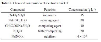
The electroless deposition was performed at 40, 50 and 60 ºC, to investigate and validate the effect of the temperature on the film formed. Figure 1 shows the scheme of electroless deposition of Ni-P onto Al2O3 particles using the surface treatment.
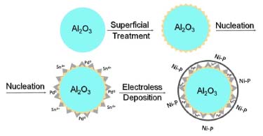 Figure 1. Illustrative scheme of Ni-P deposition on the surface alumina
Characterization The surface wettability of the Al2O3 were evaluated before and after pre-treatment by a contact angle system, model OCA 15 plus, (Dataphysics Instrument GmbH, Filderstadt, Germany). Scanning electron microscopy (SEM) analyzes were performed at Vinca Institute in Belgrade at high resolution SEM (FEI SCIOS 2 Dual Beam microscope). To enhance the SEM images and get higher energy and magnification, a very thin layer of Au was deposited on the Ni-P surface. Profilometer DekTak XT (Bruker, Billerica, USA, scan 300 µm, velocity of 20 s) were used for characterization. Atomic force microscopy (AFM) analysis was performed at Nanosurf FlexAFM model C3000. To measure the sample roughness after wet treatment and the Ni-P thin film deposition rate, a negative image of the metallic lines as shown in Figure 2 was defined by lithography using a thick resist (AZ 4620, Merck, Darmstadt, Germany) carried out at 90 ºC for 5 minutes. After exposure on a direct laser writer ("maskless lithography"), carried out through the MicroWriter model ML3 PRO (Durham Magneto Optics Ltd, London, Cambridge), the development of resist occurs by using MIF 400 K (1:4 Merck, Darmstadt, Germany) at 25 ºC. The resist that has not been developed on metallic lines was cured using a hot plate at constant temperature 120 ºC, during 20 minutes. The Ni-P layers were etched in a solution containing HNO3 (62-70% ACS, J.T. Baker, New Jersey, USA) and H3PO4 (P.A., Merck, Darmstadt, Germany) solution 9:1 (vol %) at 50 ºC.
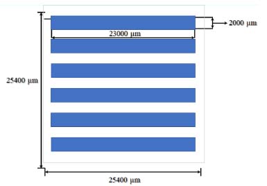 Figure 2. Layout of sample obtained by the photolithography process
RESULTS AND DISCUSSION Surface treatment Seeds for deposition are necessary on the inert substrate for the electroless plating deposition. These seeds are generated by nucleation of Sn/Pd on the surface of alumina to trigger the autocatalytic reaction in the electroless Ni-P bath. The most common procedures for nucleation consist of two solutions composed of Sn and Pd ions, both in acid chloride solution. The Sn ions anchoring in the micro pores of the Al2O3, in contact with Pd ions, reduce these ions to finely divided metallic Pd nuclei on the surface of the substrate.2,35 There are no metallic bonds between the Al2O3 and Ni-P coating, but unstable mechanical combination. So, pre-treatment is carried out to increase the micro roughness of the surface and to obtain a hydrophilic substrate in order to acquire good coatings adhesion on the Al2O3 substrate.36 To have a qualitative assessment of whether there was a change in the behavior on the Al2O3 surface after pre-treatment, surface wettability was evaluated by a contact angle. Figure 3a showed that the surface of the polished Al2O3 prior to the treatment was very hydrophobic, so the drop of water practically did not spread on the polished Al2O3 surface, presenting a contact angle of ca. 89º, unlike the treated Al2O3 surface (Figure 3b) which was quite hydrophilic. After the acidic wet treatment, the contact angle was approximately 21º, and the drop greatly spread on the treated surface.
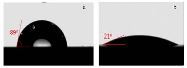 Figure 3. Contact angle images of the alumina surfaces (a) before and (b) after the wet treatment
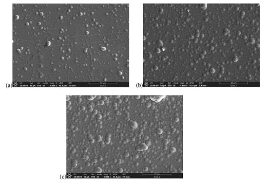
Characterization of Ni-P film deposited at different temperatures As temperature is a key factor in the electroless deposition we have prepared three samples in different temperatures (40, 50 and 60 ºC). At 30 ºC, it was not observed any deposition. The characterization by SEM of Ni-P film deposited using different temperature depositions aimed to evaluate the syntheses behavior, as can be observed in Figure 4.
The temperature affects the nucleation mechanism, consequently, it affected the Ni-P grain size deposited on the Al2O3 surface. As can be observed, there is the formation of bigger grain sizes with higher temperatures. In other words, for Ni-P films obtained at 60 ºC, the grain size was a few hundred nanometers, which ended up influencing the roughness of the film, one of the most sensitive parameters in the manufacture of devices. On the other hand, for Ni-P films deposited at 40 ºC, the grain size is much smaller, resulting in denser and more homogeneous films. For example, in the electronic area, to obtain circuits with devices containing structures of a few micrometers, it is important that the size of the particles and the roughness are smaller than the dimensions of the project. So, 40 ºC was defined as the optimized temperature for deposition and used in the further characterizations. This choice agrees with results previously obtained in our work group.37 Roughness and thickness measurements Figure 5 shows the thickness of the Ni-P film deposited by electroless autocatalytic process on the polished Al2O3 after wet treatment in different deposition times. The deposition rate of the Ni-P thin film was obtained by a linear regression and it indicates a thin film deposition rate of approximately 13.5 nm min-1. The average deposition rate is 22 nm min-1, and between these two values, we concluded that the effective deposition rate is approximately 18 nm min-1.
 Figure 5. Deposition rate of Ni-P film at 40 ºC
The graphs obtained using the equipment profilometer DEKTAK showing the roughness of Al2O3 before and after wet treatment, and the behavior of Ni-P film morphology deposited by electroless process at 40 ºC on the treated Al2O3 are shown on Figure 6.
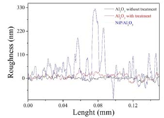 Figure 6. The profile graphic showing the surface roughness over tree different morphology
Figure 6 shows the morphology in three different situations: the Al2O3 surface without treatment (black), with chemical treatment (red) and after electroless Ni-P deposition (blue). It can be seen that after the treatment, the average roughness (10 nm) on the surface is slightly bigger than the roughness of untreated Al2O3 (5 nm) indicating that there was a change in the morphology on the Al2O3 surface. This result confirmed the analysis of the contact angle (Figure 3). It is also observed that the average roughness after the thin film deposition of Ni-P is about of 50 nm, which configures the formation of a growth of small grains. After Ni-P deposition, it can be seen that the peaks width is bigger. One of the possibilities is that, during the nucleation, regions on the surface present greater agglomeration of Pd metallic, causing a greater density of the Ni-P alloy and when the profilometer stylus probe goes around these clusters, the opening of the peaks is observed. A similar behavior can be seen after the chemical treatment of the Al2O3 surface, through the increase in roughness, the peak presents larger contours due to the bigger cavities formed. Adhesion The most common test used for evaluating coating "adhesion" is the tape-and pull-test, which has been used since the 1930's. In its simplest version, a piece of adhesive tape is pressed against the film and the resistance and degree of film removal is observed when the tape is pulled off, and an intact film with appreciable adhesion is not removed at all. So, to evaluate the Ni-P adhesion qualitatively, it was also performed a pull strength test using 3M adhesive tape (known commercially as 3M scotch 33 + electrical tape), which was compressed to remove residual air and pulled. This procedure was performed according to ASTM D335938 and also according to Campos et al.24 After the pull test, it was observed that no residues from the deposited film were attached on the tape (Figure 7), indicating a strong adherence. This means that the surface treatment was effective and a good adhesion between metal layer and alumina was achieved.
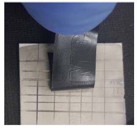 Figure 7. Peeling off tape from Ni-P film on cross-cut test
At the present moment, there is no test that can precisely assess the actual physical strength of an adhesive bond. However, it can also be said that the thin film of Ni-P after wet treatment of alumina obtained a relative adhesion performance. Surface morphology The surface morphology of Ni-P at 40 ºC deposits employed by SEM (Figure 2S, supplementary material) showed homogeneous coating over the Al2O3 surface area, with particles size smaller than 1 µm of Ni-P deposited on a smooth surface, forming a thin nanostructured film. It can be seen in Figure 2S that the growth of the thin film is quite compact, without cracks and holes. It is observed in Figure 2S(b) that the metallic thin film is formed presenting a spherical shape and the average size of these spheres is smaller than 1 µm. Figure 8 shows images obtained by AFM of Ni-P thin film plating on Al2O3; the results are similar of what was found from SEM and perfilometer analyzes.
As the purpose of the project was to obtain metallic structures with dimensions of a few microns, to be used in the electronic area, it is important that the alumina is polished and the Ni-P film deposited by the electroless method grows uniformly without holes and cracks (Figure 8 and Figure 2S(a)) and also do not form agglomerates with areas of micrometric dimensions (Figure 8 and Figure 2S(b)) that could interfere with the metallic structures. The EDS analysis was performed on the Ni-P thin film (Figure 9). The results showed that the majority of the film was formed with Ni with a P content of ca. 10%. The image represented by colors (Figure 9b) shows that there is no formation of self-cluster agglomeration of the same element, indicating a uniform and proportional distribution of the elements (C, P, Ni, O) on the film after the electroless Ni-P deposition.
 Figure 9. EDS quantification (a) and element distribution (b) of electroless Ni-P deposition over Al2O3 substrate
CONCLUSIONS From the results obtained in this study, we can conclude that the metallization of high purity and polished Al2O3 substrate (99.6%) was established based on the autocatalytic electroless technique of film deposition. The use of this type of substrate obtains Ni-P film with good morphology, with low roughness (lower than 50 nm) and, as a result, the thin film growth is quite compact, leading to no cracks and holes in the thin film formation. The results showed that the treatment of the polished Al2O3 with 0.4% of vitreous materials presented a high-performance depositing film at a low temperature (40 ºC) with a compact and continuous film with small grain size, and low roughness. The temperature affects the nucleation, with formation of bigger grain sizes at higher temperatures, therefore 40 ºC was defined as the optimized temperature for deposition and used in the further characterizations. We also observed that after the pull strength test using adhesive tape, no residues from the Ni-P deposit film were attached to the tape. This indicated a good adhesion, providing its use for electronic circuits applications. The process permits the development of a full wet Ni-P deposition process and shows an excellent alternative to obtain a Ni-P thin film with a low-cost process compared to other methods.
SUPPLEMENTARY MATERIAL Supplementary information is freely available at http://quimicanova.sbq.org.br, in PDF format.
ACKNOWLEDGEMENTS The authors thank the Assembly, Packaging and System Integration Division (DIMES) and Renato Archer Center for Information Technology (CTI), by the opportunity to use the facilities and equipment. The authors also thank the National Council for Scientific and Technological Development (CNPq) for financial support of this research. The authors are sincerely grateful to Rosalva dos Santos Marques (CTI) for SEM observations and EDS analysis.
REFERENCES 1. Schlesinger, M. In Modern Electroplating; Schlesinger, M.; Pauvonic, M., eds.; John Wiley and Sons: Hoboken, 2010, ch. 18. 2. Khoperia, T. N.; Microelectron. Eng. 2003, 69, 391. [Crossref] 3. Hari Krishnan, K.; John, S.; Srinivasan, K. N.; Praveen, J.; Ganesan, M.; Kavimani, P. M.; Metall. Mater. Trans. A 2006, 37, 1917. [Crossref] 4. Flacker, A.; Gomes, C. G.; Silva, O. M.; Teixeira, C. R.; J. Braz. Chem. Soc. 2022, 33, 600. [Crossref] 5. Shacham-Diamand, Y.; Osaka, T.; Okinaka, Y.; Sugiyama, A.; Dubin, D.; Microelectron. Eng. 2015, 132, 35. [Crossref] 6. Sullivan, M. T.; Eigler, H.; J. Electrochem. Soc. 1975, 104, 226. [Link] accessed in May 2023 7. Kobayashi, T.; Ishibashi, J.; Mononobe, S.; Ohsu, M.; Honma, H.; J. Electrochem. Soc. 2000, 147, 1046. [Crossref] 8. Khoperia, T. N.; Zedginidze, T. L.; ECS Trans. 2008, 11, 87. [Crossref] 9. Hsu, H. H.; Lin, K. H.; Lin, S. J.; Yeh, J. W.; J. Electrochem. Soc. 2001, 148, C47. [Crossref] 10. Li, J.; O'Keefe, J.; M.; O'Keefe, T. J.; Surf. Coat. Technol. 2011, 205, 3134. [Crossref] 11. Honma, H.; Kobayashi, T.; J. Electrochem. Soc. 1994, 141, 730. [Crossref] 12. Furukava, S.; Mehregany, M.; Sens. Actuators, A 1996, 56, 261. [Crossref] 13. Marques, A. E. B.; Santos Filho, S. G.; Martini, S.; Phys. Status Solidi C 2007, 4, 256. [Crossref] 14. Costa, S. J.; Flacker, A.; Nakashima, S. H. M.; Fruett, F.; Zampiere, M.; Longo, E.; ECS Trans. 2012, 49, 451. [Crossref] 15. Finardi, A. C.; Ponchet, F. A.; Adamo, B. C.; Flacker, A.; Teixeira, C. R.; Panepucci, R. R.; Mater. Res. Express 2017, 4, 36305. [Crossref] 16. Adamo, B. C.; Flacker, A.; Cavalcanti, M. H.; Teixeira, C. R.; Rotondaro, L. P. A.; Manera, T. L.; Journal of Integrated Circuits and Systems 2016, 11, 19. [Link] accessed in April 2023 17. Flacker, A.; Adamo, B. C.; Teixeira, C. R.; Tratamento de Superfície 2015, 194, 42. [Link] accessed in April 2023 18. Balaraju, J. N.; Narayanan, T. S. N. S.; Seshadri, S. K.; J. Appl. Electrochem. 2003, 33, 807. [Link] accessed in April 2023 19. Lelevic, A.; Arxiv 2018. [Crossref] 20. Huang, Z.; Nguyen, T. T.; Zhou, Y.; Qi, G.; Surf. Coat. Technol. 2019, 372, 160. [Crossref] 21. Parameswaran, M.; Xie, D.; Glavina, G. P.; J. Electrochem. Soc. 1993, 140, L111. [Link] accessed in May 2023 22. Mayers, R. H.; Plat. Surf. Finish. 1999, 5, 60. [Link] accessed in May 2023 23. O'Sullivam, M. J. E.; Horkans, J.; White, R. J.; Roland, M. J.; IBM J. Res. Dev. 1988, 32, 591. [Link] accessed in May 2023 24. Natividad, E.; Lataste, E.; Lahaye, M.; Heintz, J. M.; Silvain, J. F.; Surf. Sci. 2004, 557, 129. [Crossref] 25. CoorsTek; Thin-Film Ceramic Substrates Design Guide, 2011, available at https://www.coorstek.com/media/4222/thin-film-ceramic-substrates-design-guide.pdf, accessed in April 2023. 26. Campos, C. D. M.; Flacker, A.; Moshkalev, A. S.; Nobrega, G. O. E.; Thin Solid Films 2012, 520, 4871. [Crossref] 27. Zhang, P.; Lv, Z.; Liu, X.; Xie, G.; Zhang, B.; Catal. Commun. 2021, 149, 106238. [Crossref] 28. Volpe, M.; Inguanta, R.; Piazza, S.; Sunseri, C.; Surf. Coat. Technol. 2006, 200, 5800. [Crossref] 29. Honma, H.; Kanemitsu, K.; Plat. Surf. Finish. 1987, 15, 62. [Link] accessed in May 2023 30. Gan, X.; Zhou, K.; Hu, W.; Zhang, D.; Surf. Coat. Technol. 2012, 206, 3405. [Crossref] 31. Tsai, K. T.; Chao, G. C.; Appl. Surf. Sci. 2004, 233, 180. [Crossref] 32. Beygi, H.; Saijadi, S. A.; Zebarjad, S. M.; Appl. Surf. Sci. 2012, 261, 166. [Crossref] 33. Yamagishi, K.; Okamoto, N.; Mitsumata, N.; Fukumuro, N.; Yae, S.; Matsuda, H.; Trans. Inst. Met. Finish. 2004, 4, 82. [Crossref] 34. Campos, M. D. C.; Flacker, A.; Vaz, R. A.; Moshkalev, A. S.; Nobrega, O. G. E.; J. Electrochem. Soc. 2011, 158, D330. [Crossref] 35. Ozaki, T.; Zhang, Y.; Komaki, M.; Nishimura, C.; Int. J. Hydrogen Energy 2003, 28, 297. [Crossref] 36. Ma, H.; Liu, Z.; Wu, L.; Wang, Y.; Wang, X.; Thin Solid Films 2011, 519, 7860. [Crossref] 37. Vidal, M. M.; Flacker, A.; Teixeira, R. C.; Journal of Integrated Circuits Systems 2020, 15, 1. [Crossref] 38. American Society for Testing and Materials (ASTM); ASTM D3359: Standard Test Methods for Measuring Adhesion by Tape Test, 2009. [Link] accessed in May 2023 |
On-line version ISSN 1678-7064 Printed version ISSN 0100-4042
Qu�mica Nova
Publica��es da Sociedade Brasileira de Qu�mica
Caixa Postal: 26037
05513-970 S�o Paulo - SP
Tel/Fax: +55.11.3032.2299/+55.11.3814.3602
Free access


